
In the electronics industry, plasma has already been adopted in electronics, PCB, and semiconductor manufacturing to improve adhesion for Anisotropic Conductive Film (ACF) in flat panel display assembly, manufacture silicon photovoltaic cells, and bond polymers with adhesives. Additional applications include enhancing the performance of inks, dyes, potting materials, over-molding, and under-fill compounds. Plasma can also be used for surface cleaning of wire and die bond pads and gold-plated contact points to improve connections.
Plasma is a state of matter, like a solid, liquid, or gas. When sufficient energy is applied to a gas, it becomes ionized, transitioning into the plasma state.
“With precise application and control, plasma can alter surface properties of printed circuit board PCB and electronic components without compromising the underlying material. These techniques can boost the bond strength by up to 50 times in certain cases,” says Ryan Blaik, Sales Manager of Corona-based PVA TePla.
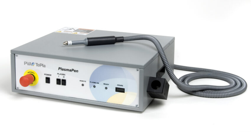
While there are multiple methods for applying plasma to a product’s surface, one of the most popular and accessible are plasma “pens.” These tools ionize gas, such as air or noble gases, under normal, atmospheric, pressure conditions using electrical discharges.
“The plasma produced from the tip of the pen can be applied to very specific areas, or the entire part,” explains Blaik, adding that often plasma pens are incorporated into automated inline manufacturing processes or controlled by robots.
Today, plasma pens are being used to solve various electronics adhesion challenges:
• For most electronics applications, plasma treatments are utilized to increase the surface free energy of the material. When a substrate has high surface energy, adhesives and other liquids often spread more easily across the surface. There are several mechanisms for increasing surface energy with plasma, including precision cleaning, chemically or physically modifying the surface, increasing surface area by roughening, and by applying primer coatings.
• The plasma pen is particularly effective for preparing materials in overmolding processes, including polypropylene applications, dip coatings, or any method that involves encasing or encapsulating components. A common application of silicone overmolding is to safeguard electronic boards against exposure to outdoor weather conditions.
• Plasma generated from atmospheric air exhibits strong oxidative properties, making it highly effective for surface cleaning and activation. Layers of absorbed molecules, such as oil and water on metallic surfaces, can be easily removed to improve adhesion.
• Atmospheric plasma can also be used to oxidize the surface of plastics to promote adhesion of materials like inks, adhesives, or coatings.
Although plasma pens follow a standard design, significant variations exist between different models. Manufacturers like PVA TePla provide various options and customizations to meet specific needs, including adjustments to the aspect ratio of the plasma plume, intensity, and dwell times.
For more information, contact PVA TePla America at 800-527-5667, visit www.pvateplaamerica.com, or email ryanb@pvateplaamerica.com.