
Plasma is a state of matter, like a solid, liquid, or gas. When sufficient energy is applied to a gas, it becomes ionized, transitioning into the plasma state. With precise application and control, plasma can alter surface properties of a metal or plastic part without compromising the underlying material.
Although plasma has a wide range of applications, it is frequently used to improve the adhesion of chemical glues, printing inks, and coatings. This is often the best – and only – solution for manufacturers facing persistent challenges such as high failure rates caused by delamination, inadequate bonding, poor surface printing, or issues with coating adhesion.
“Plasma contains ions, electrons, neutral particles, and reactive species that can be utilized for precision cleaning, decontamination, increasing surface “wettability,” and other surface modifications. These techniques can boost the bond strength by up to 50 times in certain cases,” says Ryan Blaik, Sales Manager of Corona-based PVA TePla.
While there are multiple methods for applying plasma to a product’s surface, one of the most popular and accessible are plasma “pens.” These tools – which ionize gas such as air or noble gases under normal atmospheric pressure conditions using electrical discharges – provide various advantages:
• The plasma produced from the tip of the pen can be applied to very specific areas, or the entire part.
• Plasma pens serve as an affordable introduction to plasma technology. For manufacturers that only need to spot treat a part or operate high-speed production lines, a solution as simple and affordable as a pen may make more sense than a larger, more costly, batch processing system.
• Plasma pens not only reduce upfront investment but also simplify exhaust management and are suitable for smaller-scale production requirements.
• Unlike traditional vacuum-based plasma chambers where parts are processed in high volume batches, plasma pens can be installed inline, require less energy, and incur lower operational costs.
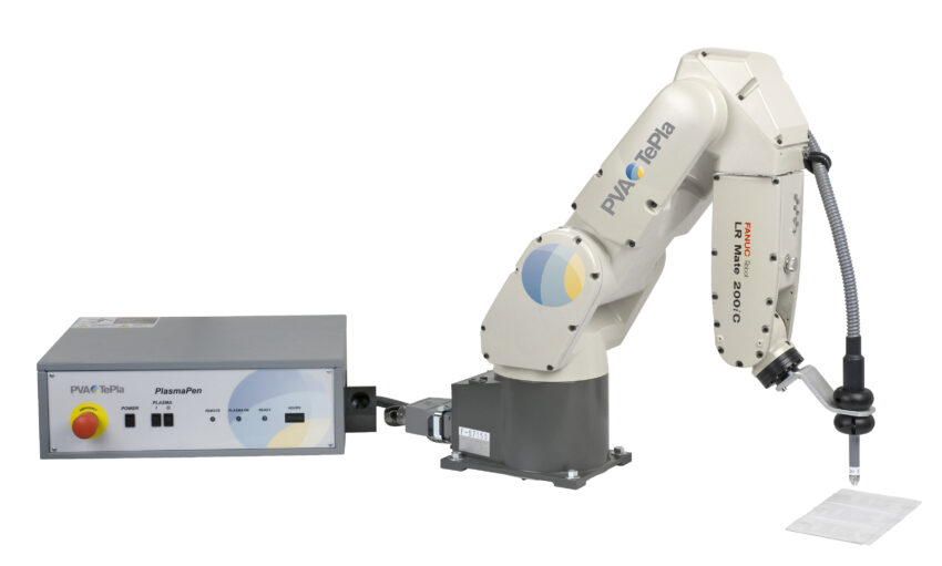
• Plasma pens can also be incorporated into automated inline manufacturing processes or controlled by robots when required.
Today, plasma pens have already been adopted in the automotive, aerospace, electronics, medical devices, and packaging industries. Current uses include improving adhesion for Anisotropic Conductive Film (ACF) in flat-panel display assembly, manufacturing silicon photovoltaic cells, assembling thin-film photovoltaic modules, and bonding polymers with adhesives. Additional applications include enhancing the performance of inks, dyes, paints, potting materials, over-molding, under-fill compounds, and various biomaterials.
For more information, contact PVA TePla America at 951-371-2500 or 800-527-5667, ryanb@pvateplaamerica.com or visit www.pvateplaamerica.com.