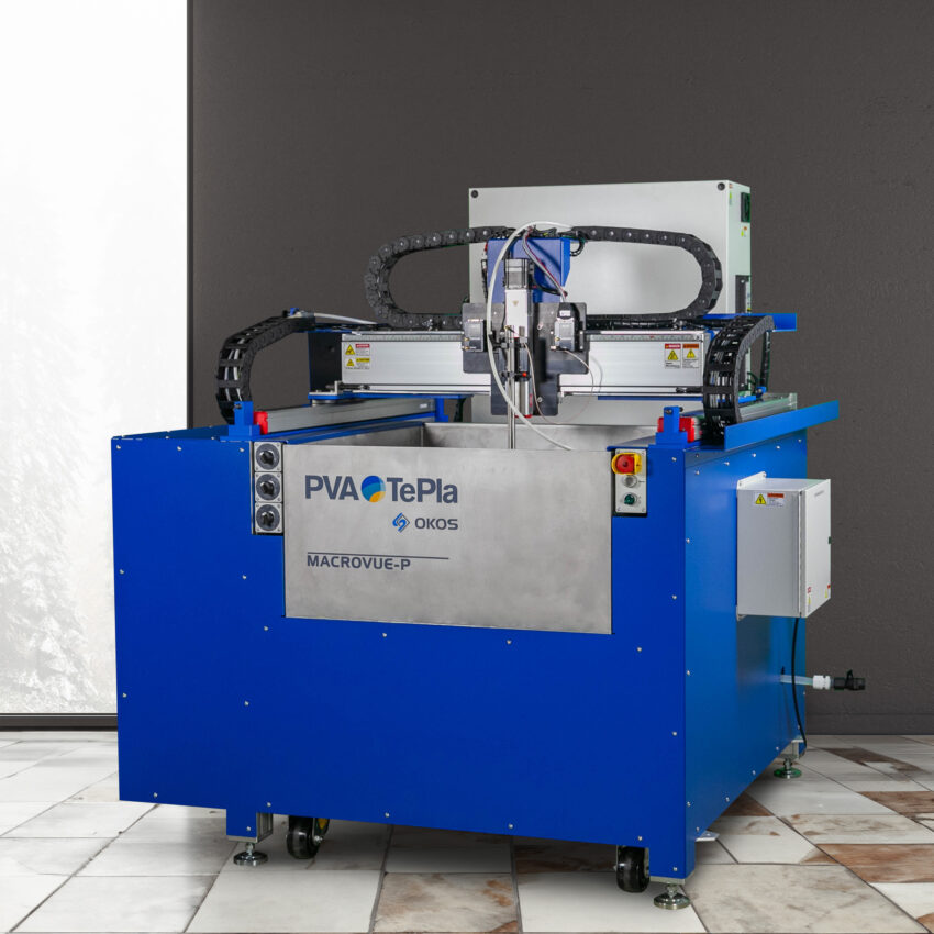
To meet ever increasing demand for silicon carbide (SiC) crystals, the world needs much higher yields without sacrificing quality. Today, SiC crystals are crucial in the manufacture of smaller, faster, more efficient chips and power electronics systems. However, without advanced metrology tools capable of promptly detecting minor flaws, the SiC crystal growing sector essentially operates blindly, resulting in unacceptable defects and costly product losses.
With the silicon carbide production industry still in its nascent stages, those driving innovation to achieve a competitive edge and deliver high-yield, reliable products must conduct defect testing throughout all production phases. Utilizing advanced metrology methods, such as Scanning Acoustic Microscopy (SAM), becomes crucial for defect identification, elimination, and process optimization.
SAM, a non-invasive, non-destructive, ultrasonic testing method capable of highspeed 100% testing, is already the industry standard for 100% inspection of semiconductor components for identifying defects within microelectronic devices.
“If the final product cannot be inspected, it becomes challenging to identify potential imperfections in the SiC crystals and pinpoint the stage of the process where issues may have arisen. Possible causes could include material defects, temperature fluctuations, or problems within the hot zone. Advanced metrology equipment like SAM can help crystal growers detect minute flaws, defects, and map these [into their process variation] to correct any problems going forward,” says Hari Polu, President of OKOS, a Virginia-based manufacturer of SAM and industrial ultrasonic non-destructive (NDT) systems. The company serves the SiC crystal growing, chip fabrication, electronics, aerospace, metal/alloy/composite manufacturing, and end-user markets.
SAM Enables Rapid, High-Resolution SiC Defect Detection
“Advanced SAM systems make it possible to move to a higher level of failure analysis because of the level of detection and precision involved. In the past, detecting a 500-micron defect was the goal; now it is a 50-micron defect. With this type of testing, we can inspect materials and discover flaws that were previously undetected,” says Polu.
In fact, SAM seems to address at least one of the elements identified by the National Institute of Standards and Technology (NIST) as necessary for the U.S. to lead the global semiconductor manufacturing industry once again.
NIST’s recent report titled Strategic Opportunities for U.S. Semiconductor Manufacturing identifies 7 Grand Challenges that need critical attention from a metrology perspective to achieve the vision of a U.S.-led global semiconductor industry. In addition, the report identifies 32 Path Forward Elements that describe potential strategies for addressing the challenges.
For one of the grand challenges, Advanced Metrology for Future Micro-electronics Manufacturing, SAM essentially answers one of the Path Forward Elements, namely “rapid, high-resolution, non-destructive techniques for characterizing defects and impurities and correlating them with performance and reliability.”
For more information, contact OKOS at info@okos.com or visit www.okos.com. OKOS is a wholly owned subsidiary of PVA TePla AG, Germany.

