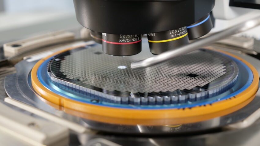
To improve quality control and prevent the packaging of faulty chips in crucial electronic devices like today’s intelligent vehicles, the semiconductor sector is concentrating on automating the few remaining manual tasks in wafer processing.
“Although the process equipment used in semiconductor fabs is extremely sophisticated, there are still manual tasks involved that could benefit from automation standards. A prime example is in wafer dicing, where the commonly practiced manual inspection of sawed wafers is very often lacking digital traceability. By rectifying these minor gaps in the process, the industry can improve quality control and auditing of diced wafers prior to packaging,” says Kevin Fredriksen of PVA Software Production Automation (SPA), a company that offers complete high-precision measurement and inspection systems of wafers for the semiconductor industry.
Now, new technology is closing the gaps between sawing, inspection, and inking through improved automation and inspection with instruments like SPA’s MI3061 automatic visual microscope for wafer inspection up to 300 mm in size. The inspection process begins with the operator taking the wafer on frame out of the sawing machine and placing it onto a vacuum transmitted light chuck that holds the frame. The operator triggers the movement of the XY stage with a one-click start. Afterwards the frame label is automatically positioned under the reader where the ID code is read. It starts the lot and loads the correct product recipe and wafer map.
To ensure that the chip position and the corresponding wafer map are synchronized, the system features an automatic alignment and expansion compensation procedure. This automatic function accounts for the expansion of the wafer, which occurs during sawing and can cause a displacement of the XY chip positioning.
Once this step is completed, the wafer type recipe is used to determine which chip positions should be inspected on the wafer’s front side. After the alignment, the operator is guided through the software to proceed through additional steps in the predefined sequence, including inspecting the chip’s edges. The process is automated but can be controlled by joystick with manual focusing if necessary.
To differentiate between a loose particle and a real mechanical problem the operator can execute an air knife, which is a thin metal pipe that uses compressed air to blow off loose particles precisely from the current inspection position without touching the wafer itself. Instead of viewing the sample through the microscope, the image is displayed on a 27” monitor to simplify detection of any defects. Each of these steps can be applied to inspect the backside of the wafer (through the dicing tape), as well.
After backgrinding, defects such as scratches, cracks, and pits can negatively impact the performance and reliability of fabricated semiconductor devices. SPA actively develops and employs advanced algorithms and even artificial intelligence (AI) within customized machine projects to distinguish between defects and normal expected issues, which can be challenging to differentiate. If a defect is found, the operator can categorize it using specific error codes which are translated into bincodes in the uploaded wafer map. These codes will then initiate various subsequent actions such as navigating around scratches to guarantee all impacted chips are digitally marked, elevating the chip sample size, or progressing to a 100% wafer inspection.
Images of the defective chips are saved and included in a KLARF wafer map output file. On modern microscopes like the MI3061 applying defect information to dies is done digitally by keying in the error code while inspecting the sample. With the automatic visual microscope, complete digital traceability is provided by reporting the wafer ID, the recipe name, bincode changes and inspected chip coordinates in a log summary file. This is complemented by a SECS/GEM interface to the host.
The MI3061 compliments Advanced Visual Inspection (AVI) inspection, with some semiconductor fabs utilizing the SPA wafer inspection system to reload the result wafer maps to reinspect or review errors the system cannot classify. To simplify this process, the microscope can automatically move specific chip locations or bincodes into the field of view to inspect unclassifiable anomalies detected by the AVI machine at higher magnification. These errors can be engineered by taking photos and reclassifying the bincode number. This applies to the front and backside of the wafer.
Once wafer inspection on the microscope is complete, the wafer map is sent to the SPA Frame-Inker, a machine that automatically inks the defective wafers and performs a hundred percent ink dot inspection inside the machine. The framed wafer can then be processed correctly by the pick & place machines, leaving only the skeleton wafer that contains all failed dies.
To assure that no fail chip is accidentally picked up for subsequent processing to packaging, SPA offers a software called PickMapFirewall that overlays an image of the skeleton wafer over the actual skeleton wafer map. An exact match indicates that no defective chips were accidentally picked and postprocessed.
For more information regarding Advanced Visual Inspection, Czochralski (CZ) growers, Scanning Infrared Dipolar Inspection, or Plasma Ashing, call Bill Marsh at PVA TePla America at 951-371-2500; email sales@pvateplaamerica.com, or visit www.pvateplaamerica.com.

