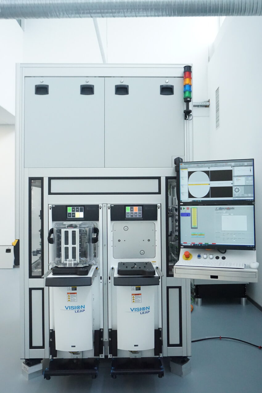
Today, hybrid bonding is transforming the semiconductor industry by facilitating the production of increasingly intricate, efficient, and powerful electronic devices. This advancement is beneficial for artificial intelligence, high-performance computing, and graphics processing units. However, to successfully transition to high volume manufacturing with high yields requires advanced metrology tools that can quickly identify defects like cracks and voids within the bonded layers.
The concept behind three-dimensional advanced packaging is to stack multiple dies or wafers vertically to achieve better performance with lower power requirements, smaller size and lower cost. However, as three-dimensional packages become increasingly complex, so do the challenges in identifying defects within vertically stacked, multiple layers.
Now, the focus is shifting to methods of non-destructive testing like Scanning Acoustic Microscopy. Scanning Acoustic Microscopy (SAM) is a non-invasive and non-destructive ultrasonic testing method that is quickly becoming the preferred technique for testing and failure analysis involving stacked dies or wafers. SAM is already the industry standard for 100% inspection of semiconductor components to identify defects such as voids, cracks, and delamination within microelectronic devices. The technology has been adapted to facilitate 100% inspection of hybrid bonded packages.
“Innovations in the design of wafer chucks, array transducers, and AI-based analysis of inspection data are converging to provide a more robust SAM solution for fabs involved in hybrid bonding,” says Hari Polu, President of PVA TePla OKOS, a Virginia-based manufacturer of SAM and industrial ultrasonic non-destructive (NDT) systems. The company serves the semiconductor, electronics, aerospace, metal/alloy/composite manufacturing, and end-user markets.
“With conventional SAM techniques, wafers were held horizontally in a chuck and processed in a water medium, and this occasionally could lead to water ingress, trapping water, which could cause significant issues in the next step of assembly. By re-designing the chuck in a vertical orientation, we can use gravity to eliminate any concern over water ingress, along with other water management technologies,” explains Polu.
Advancements in AI-based analysis of the data collected from SAM inspection of wafer-to-wafer hybrid bonding will further automate quality assurance and increase fab production.
When fabs take advantage of the higher level of failure detection and analysis, the production yield and overall reliability of high-performance chips improve significantly. Every fab will eventually move towards this level of failure analysis because of the level of detection and precision required for hybrid bonding.
For more information, contact PVA TePla OKOS at info@okos.com or visit www.okos.com.

